
Page 28 - Read Online
P. 28
Dang et al. Chem Synth 2023;3:14 https://dx.doi.org/10.20517/cs.2022.33 Page 9 of 20
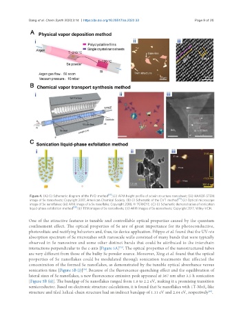
Figure 4. (A) (i) Schematic diagram of the PVD method [57] ; (ii) AFM height profile of a twin structure nanosheet; (iii) HAADF-STEM
image of Se nanosheets; Copyright 2017, American Chemical Society. (B) (i) Schematic of the CVT method [71] ; (ii) Optical microscope
image of Se nanoflakes; (iii) AFM image of a Se nanoflake; Copyright 2018, © TÜRKİYE. (C) (i) Schematic demonstration of sonication
liquid-phase exfoliation method [58] ; (ii) TEM images of Se nanosheets; (iii) AFM images of Se nanosheets; Copyright 2017, Wiley-VCH.
One of the attractive features is tunable and controllable optical properties caused by the quantum
confinement effect. The optical properties of Se are of great importance for its photoconductive,
photovoltaic and rectifying behaviors and, thus, its device application. Filippo et al. found that the UV-vis
absorption spectrum of Se microtubes with nanoscale walls consisted of many bands that were typically
observed in Se nanowires and some other distinct bands that could be attributed to the interchain
interactions perpendicular to the c-axis [Figure 5A] . The optical properties of the nanostructured tubes
[72]
are very different from those of the bulky Se powder source. Moreover, Xing et al. found that the optical
properties of Se nanoflakes could be modulated through sonication treatments that affected the
concentration of the formed Se nanoflakes, as demonstrated by the tunable optical absorbance versus
[58]
sonication time [Figure 5B (i)] . Because of the fluorescence quenching effect and the equilibration of
lateral sizes of Se nanoflakes, a new fluorescence emission peak appeared at 367 nm after 3.5 h sonication
[Figure 5B (ii)]. The bandgap of Se nanoflakes ranged from 1.8 to 2.2 eV, making it a promising transition
semiconductor. Based on electronic structure calculations, it is found that Se nanoflakes with 1T-MoS -like
2
[60]
structure and tiled helical-chain structure had an indirect bandgap of 1.11 eV and 2.64 eV, respectively .