
Page 255 - Read Online
P. 255
Keeney et al. Microstructures 2023;3:2023041 https://dx.doi.org/10.20517/microstructures.2023.41 Page 3 of 15
[43,59]
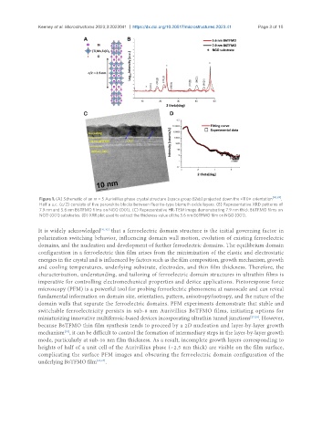
Figure 1. (A) Schematic of an m = 5 Aurivillius phase crystal structure (space group B2eb) projected down the <110> orientation .
Half a u.c. (c/2) consists of five perovskite blocks between fluorite-type bismuth oxide layers. (B) Representative XRD patterns of
7.9 nm and 5.6 nm B6TFMO films on NGO (001). (C) Representative HR-TEM image demonstrating 7.9 nm thick B6TFMO films on
NGO (001) substrates. (D) XRR plot used to extract the thickness value of the 5.6 nm B6TFMO film on NGO (001).
It is widely acknowledged [31,32] that a ferroelectric domain structure is the initial governing factor in
polarization switching behavior, influencing domain wall motion, evolution of existing ferroelectric
domains, and the nucleation and development of further ferroelectric domains. The equilibrium domain
configuration in a ferroelectric thin film arises from the minimization of the elastic and electrostatic
energies in the crystal and is influenced by factors such as the film composition, growth mechanism, growth
and cooling temperatures, underlying substrate, electrodes, and thin film thickness. Therefore, the
characterization, understanding, and tailoring of ferroelectric domain structures in ultrathin films is
imperative for controlling electromechanical properties and device applications. Piezoresponse force
microscopy (PFM) is a powerful tool for probing ferroelectric phenomena at nanoscale and can reveal
fundamental information on domain size, orientation, pattern, anisotropy/isotropy, and the nature of the
domain walls that separate the ferroelectric domains. PFM experiments demonstrate that stable and
switchable ferroelectricity persists in sub-8 nm Aurivillius B6TFMO films, initiating options for
miniaturizing innovative multiferroic-based devices incorporating ultrathin tunnel junctions [27,28] . However,
because B6TFMO thin film synthesis tends to proceed by a 2D nucleation and layer-by-layer growth
[33]
mechanism , it can be difficult to control the formation of intermediary steps in the layer-by-layer growth
mode, particularly at sub-10 nm film thickness. As a result, incomplete growth layers corresponding to
heights of half of a unit cell of the Aurivillius phase (~2.5 nm thick) are visible on the film surface,
complicating the surface PFM images and obscuring the ferroelectric domain configuration of the
underlying B6TFMO film [24,27] .