
Page 259 - Read Online
P. 259
Keeney et al. Microstructures 2023;3:2023041 https://dx.doi.org/10.20517/microstructures.2023.41 Page 7 of 15
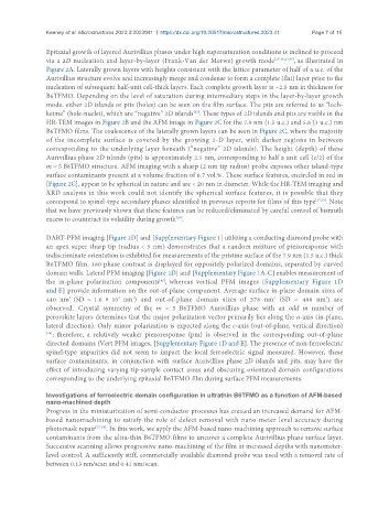
Epitaxial growth of layered Aurivillius phases under high supersaturation conditions is inclined to proceed
via a 2D nucleation and layer-by-layer (Frank-Van der Merwe) growth mode [27-30,33,45] , as illustrated in
Figure 2A. Laterally grown layers with heights consistent with the lattice parameter of half of a u.c. of the
Aurivillius structure evolve and increasingly merge and condense to form a complete (flat) layer prior to the
nucleation of subsequent half-unit cell-thick layers. Each complete growth layer is ~2.5 nm in thickness for
B6TFMO. Depending on the level of saturation during intermediary steps in the layer-by-layer growth
mode, either 2D islands or pits (holes) can be seen on the film surface. The pits are referred to as “loch-
[33]
keime” (hole-nuclei), which are “negative” 2D islands . These types of 2D islands and pits are visible in the
HR-TEM images in Figure 2B and the AFM image in Figure 2C for the 7.9 nm (1.5 u.c.) and 5.6 (1 u.c.) nm
B6TFMO films. The coalescence of the laterally grown layers can be seen in Figure 2C, where the majority
of the incomplete surface is covered by the growing 2-D layer, with darker regions in between
corresponding to the underlying layer beneath (“negative” 2D islands). The height (depth) of these
Aurivillius phase 2D islands (pits) is approximately 2.5 nm, corresponding to half a unit cell (c/2) of the
m = 5 B6TFMO structure. AFM imaging with a sharp (2 nm tip radius) probe exposes other island-type
surface contaminants present at a volume fraction of 6.7 vol.%. These surface features, encircled in red in
[Figure 2C], appear to be spherical in nature and are < 20 nm in diameter. While the HR-TEM imaging and
XRD analysis in this work could not identify the spherical surface features, it is possible that they
correspond to spinel-type secondary phases identified in previous reports for films of this type [27,28] . Note
that we have previously shown that these features can be reduced/eliminated by careful control of bismuth
[28]
excess to counteract its volatility during growth .
DART-PFM imaging [Figure 2D] and [Supplementary Figure 1] utilizing a conducting diamond probe with
an apex super sharp tip (radius < 5 nm) demonstrates that a random mixture of piezoresponse with
indiscriminate orientation is exhibited for measurements of the pristine surface of the 7.9 nm (1.5 u.c.) thick
B6TFMO film. 180 phase contrast is displayed for oppositely polarized domains, separated by curved
domain walls. Lateral PFM imaging [Figure 2D] and [Supplementary Figure 1A-C] enables measurement of
[42]
the in-plane polarization components , whereas vertical PFM images [Supplementary Figure 1D
and E] provide information on the out-of-plane component. Average surface in-plane domain sizes of
3
2
440 nm (SD = 1.6 × 10 nm ) and out-of-plane domain sizes of 378 nm (SD = 488 nm ) are
2
2
2
observed. Crystal symmetry of the m = 5 B6TFMO Aurivillius phase with an odd m number of
perovskite layers determines that the major polarization vector primarily lies along the a-axis (in-plane,
lateral direction). Only minor polarization is expected along the c-axis (out-of-plane, vertical direction)
[46] ; therefore, a relatively weaker piezoresponse (pm) is observed in the corresponding out-of-plane
directed domains (Vert PFM images, [Supplementary Figure 1D and E]. The presence of non-ferroelectric
spinel-type impurities did not seem to impact the local ferroelectric signal measured. However, these
surface contaminants, in conjunction with surface Aurivillius phase 2D islands and pits, may have the
effect of introducing varying tip-sample contact areas and obscuring orientated domain configurations
corresponding to the underlying epitaxial B6TFMO film during surface PFM measurements.
Investigations of ferroelectric domain configuration in ultrathin B6TFMO as a function of AFM-based
nano-machined depth
Progress in the miniaturization of semi-conductor processes has created an increased demand for AFM-
based nanomachining to satisfy the role of defect removal with nano-meter level accuracy during
photomask repair [37-39] . In this work, we apply the AFM-based nano-machining approach to remove surface
contaminants from the ultra-thin B6TFMO films to uncover a complete Aurivillius phase surface layer.
Successive scanning allows progressive nano-machining of the film at increased depths with nanometer-
level control. A sufficiently stiff, commercially available diamond probe was used with a removal rate of
between 0.13 nm/scan and 0.41 nm/scan.