
Page 260 - Read Online
P. 260
Page 8 of 15 Keeney et al. Microstructures 2023;3:2023041 https://dx.doi.org/10.20517/microstructures.2023.41
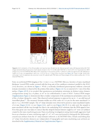
Figure 2. (A) A schematic of the 2D nucleation and layer-by-layer (Frank-Van der Merwe) growth mode. (B) Representative HR-TEM
images demonstrating the presence of 2D islands and pits in the 7.9 nm thick B6TFMO film on NGO (001). (C) Representative AFM
image of 5.6 nm thick B6TFMO film NGO (001) substrates. A line section profile 1 is shown in white through the 2D pits indicating a
height of 2.5 nm, corresponding to half a u.c. (c/2) of the m = 5 Aurivillius structure (see Figure 1A). Small circular island-type
inclusions (< 20 nm diameter) are encircled in red. (D) Lateral (Lat) PFM Amp and Phase images of the pristine surface of a 7.9 nm
thick B6TFMO film.
Next, we performed PFM imaging of the 7.9 nm (1.5 u.c.) B6TFMO film as a function of nano-machined
thickness. Lateral PFM results, scanned with the long-axis of the cantilever orientated parallel to the NGO
[010] direction, are shown in Figure 3. While a randomly distributed piezoresponse without a favored
domain orientation is observed for the pristine film surface [Figure 3A-C], on removal of 0.7 nm of the film
surface [Figure 3D-F], it is revealed that spontaneous polarization orientates in distinct stripe domain
configurations along the a-b plane, at 45° to the orthorhombic b-axis of NGO. Vertical PFM images
[Supplementary Figure 2] demonstrate that a weaker component of the spontaneous polarization exists out
of the a-b plane (along the c-axis). This observed vertical response is expected for an m = 5, an odd-layered
Aurivillius phase . The measured domain widths are of the order of 0.14 µm for the nano-machined 7.9
[47]
nm (1.5 u.c.) B6TFMO sample. The 45° stripe domains were observed to persist at nano-machined depths
of 2.0 nm [Figure 3G-I], 3.8 nm [Figure 3J-L], and 6.2 nm [Figure 3M-O]. It is only until the sample is
nano-machined all the way through the film to the underlying NGO substrate that the PFM signal is lost.
Note that great care was taken to ensure that the striped domain features angled at 45° were not artifacts
created by the nano-machining process. Nano-machining investigations using intentionally aggressive load
forces as a function of nano-machining angle (0°, 45°, 90°) were performed to distinguish the deliberately-
created scan artifacts from the 45° stripe domains inherent to the B6TFMO films. Details establishing that
45° stripe ferroelectric domains are independent of topography and nano-machining scan artifacts are
described in the Supplementary Material and Supplementary Figure 3.