
Page 262 - Read Online
P. 262
Page 10 of 15 Keeney et al. Microstructures 2023;3:2023041 https://dx.doi.org/10.20517/microstructures.2023.41
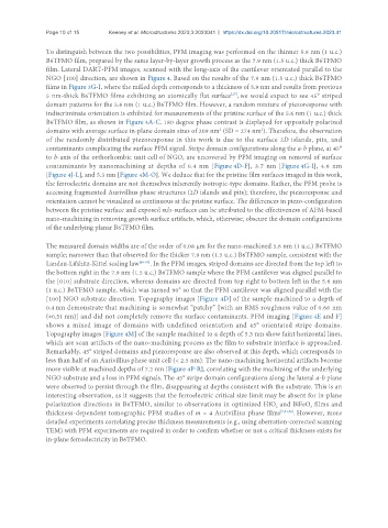
To distinguish between the two possibilities, PFM imaging was performed on the thinner 5.6 nm (1 u.c.)
B6TFMO film, prepared by the same layer-by-layer growth process as the 7.9 nm (1.5 u.c.) thick B6TFMO
film. Lateral DART-PFM images, scanned with the long-axis of the cantilever orientated parallel to the
NGO [100] direction, are shown in Figure 4. Based on the results of the 7.9 nm (1.5 u.c.) thick B6TFMO
films in Figure 3G-I, where the milled depth corresponds to a thickness of 5.9 nm and results from previous
[27]
5 nm-thick B6TFMO films exhibiting an atomically flat surface , we would expect to see 45° striped
domain patterns for the 5.6 nm (1 u.c.) B6TFMO film. However, a random mixture of piezoresponse with
indiscriminate orientation is exhibited for measurements of the pristine surface of the 5.6 nm (1 u.c.) thick
B6TFMO film, as shown in Figure 4A-C. 180 degree phase contrast is displayed for oppositely polarized
2
domains with average surface in-plane domain sizes of 209 nm (SD = 274 nm ). Therefore, the observation
2
of the randomly distributed piezoresponse in this work is due to the surface 2D islands, pits, and
contaminants complicating the surface PFM signal. Stripe domain configurations along the a-b plane, at 45°
to b-axis of the orthorhombic unit cell of NGO, are uncovered by PFM imaging on removal of surface
contaminants by nanomachining at depths of 0.4 nm [Figure 4D-F], 3.7 nm [Figure 4G-I], 4.6 nm
[Figure 4J-L], and 5.3 nm [Figure 4M-O]. We deduce that for the pristine film surfaces imaged in this work,
the ferroelectric domains are not themselves inherently isotropic-type domains. Rather, the PFM probe is
accessing fragmented Aurivillius phase structures (2D islands and pits); therefore, the piezoresponse and
orientation cannot be visualized as continuous at the pristine surface. The differences in piezo-configuration
between the pristine surface and exposed sub-surfaces can be attributed to the effectiveness of AFM-based
nano-machining in removing growth surface artifacts, which, otherwise, obscure the domain configurations
of the underlying planar B6TFMO film.
The measured domain widths are of the order of 0.08 µm for the nano-machined 5.6 nm (1 u.c.) B6TFMO
sample; narrower than that observed for the thicker 7.9 nm (1.5 u.c.) B6TFMO sample, consistent with the
Landau-Lifshitz-Kittel scaling law [48-50] . In the PFM images, striped domains are directed from the top left to
the bottom right in the 7.9 nm (1.5 u.c.) B6TFMO sample where the PFM cantilever was aligned parallel to
the [010] substrate direction, whereas domains are directed from top right to bottom left in the 5.6 nm
(1 u.c.) B6TFMO sample, which was turned 90° so that the PFM cantilever was aligned parallel with the
[100] NGO substrate direction. Topography images [Figure 4D] of the sample machined to a depth of
0.4 nm demonstrate that machining is somewhat “patchy” [with an RMS roughness value of 0.66 nm
(±0.51 nm)] and did not completely remove the surface contaminants. PFM imaging [Figure 4E and F]
shows a mixed image of domains with undefined orientation and 45° orientated stripe domains.
Topography images [Figure 4M] of the sample machined to a depth of 5.3 nm show faint horizontal lines,
which are scan artifacts of the nano-machining process as the film to substrate interface is approached.
Remarkably, 45° striped domains and piezoresponse are also observed at this depth, which corresponds to
less than half of an Aurivillius phase unit cell (< 2.5 nm). The nano-machining horizontal artifacts become
more visible at machined depths of 7.2 nm [Figure 4P-R], correlating with the machining of the underlying
NGO substrate and a loss in PFM signals. The 45° stripe domain configurations along the lateral a-b plane
were observed to persist through the film, disappearing at depths consistent with the substrate. This is an
interesting observation, as it suggests that the ferroelectric critical size limit may be absent for in-plane
polarization directions in B6TFMO, similar to observations in optimized HfO and BiFeO films and
2
3
thickness-dependent tomographic PFM studies of m = 4 Aurivillius phase films [7,51,52] . However, more
detailed experiments correlating precise thickness measurements (e.g., using aberration-corrected scanning
TEM) with PFM experiments are required in order to confirm whether or not a critical thickness exists for
in-plane ferroelectricity in B6TFMO.