
Page 25 - Read Online
P. 25
Hansen et al. Microstructures 2023;3:2023029 https://dx.doi.org/10.20517/microstructures.2023.17 Page 3 of 17
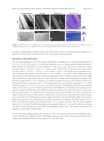
Figure 1. (A) VBF, (B) index, (C) reliability, and (D) orientation maps of the SMA sample. (E) VBF, (F) index, (G) reliability, and (H)
orientation maps of the VO on sapphire sample. Note the reliability and orientation maps are noisy in both samples.
2
automatic crystallographic mapping methods are open-source, easy to use, and less prone to human errors
and can be useful tools for researchers who work on martensitic material systems.
MATERIALS AND METHODS
The two model systems we use in this study to develop the crystallographic variant mapping methods are
(1) a Ni Ti Hf SMA and (2) a VO thin film deposited on a c-cut monocrystalline sapphire substrate.
50.3
2
20
29.7
Both samples are martensitic at room temperature. The Ni Ti Hf SMA has a monoclinic crystal
20
29.7
50.3
structure, with a = 3.052 Å, b = 4.089 Å, c = 4.887 Å, and β= 102.91 . The VO also has a monoclnic crystal
o
2
o[12]
structure, with a = 5.752 Å, b = 4.538 Å, c = 5.383 Å, and β = 122.65 . The b-axis of VO is parallel to the c-
2
axis of sapphire (hexagonal crystal structure, a = 4.760 Å and c = 12.994 Å) . The detailed processing
[24]
information of these samples can be found in our previous work [11,25] . SMAs are known for their shape
memory effect and super-elastic behavior, which make them widely used in mechanical, aerospace, and
biomedical applications [4,26] . VO undergoes an insulator-to-metal transition when heated up above the
2
phase transformation temperature and is a promising material for neuromorphic computing [27,28] . The SMA
sample was aged at 550 C for 10 h to grow nanoscale precipitates. The diffraction patterns were obtained
o
with a 200 kV FEI Tecnai F20 ST TEM equipped with a NanoMEGAS ASTAR system with a Stingray CCD
camera to acquire the PED data. The diffraction pattern acquisition rate is approximately 0.06 s per pixel.
o
o
The precession angle is 0.3 , and the electron beam spot size is approximately 3 nm. The 0.3 precession
angle was selected because it offers a good combination of reduction in the dynamical effect and retaining a
decent beam spot size. While larger precession angles can further reduce the dynamical effect, they result in
larger beam spot sizes and, consequently, poorer spatial resolution for mapping. The SMA map is 285 × 285
pixels. The diffraction patterns were acquired with a 144 × 144 pixel resolution. The VO on the sapphire
2
map is 150 × 100 pixels. The diffraction patterns were acquired with a 580 × 580 pixel resolution to evaluate
the effect of noise and denoise on the final crystallographic variant maps. The denoise was achieved by
applying a 5-pixel radius Gaussian filter.
For the PED data reading and then processing, the “.blo” file is loaded and read using Hyperspy, which
converts the file into a usable 4D array . Hyperspy is an open-source Python library that provides tools to
[29]
analyze multi-dimensional data, such as a function to read “.blo” files.