
Page 171 - Read Online
P. 171
Page 6 of 10 Ge et al. Microstructures 2023;3:2023026 https://dx.doi.org/10.20517/microstructures.2023.13
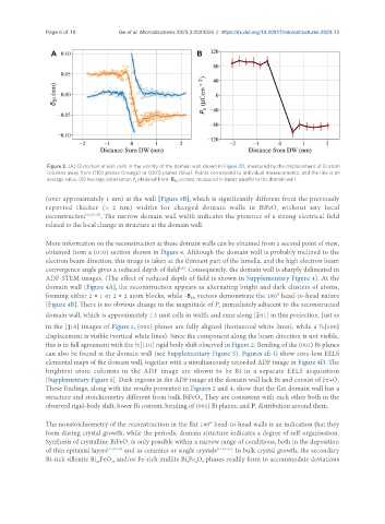
Figure 3. (A) Distortion of unit cells in the vicinity of the domain wall shown in Figure 2D, measured by the displacement of Bi atom
columns away from (110) planes (orange) or (001) planes (blue). Points correspond to individual measurements, and the line is an
average value. (B) Average polarisation P obtained from -δ vectors, measured in bands parallel to the domain wall.
FB
s
(over approximately 1 nm) at the wall [Figure 3B], which is significantly different from the previously
reported thicker (> 2 nm) widths for charged domain walls in BiFeO without any local
3
reconstruction [23,25-27] . The narrow domain wall width indicates the presence of a strong electrical field
related to the local change in structure at the domain wall.
More information on the reconstruction at these domain walls can be obtained from a second point of view,
obtained from a (010) section shown in Figure 4. Although the domain wall is probably inclined to the
electron beam direction, this image is taken at the thinnest part of the lamella, and the high electron beam
convergence angle gives a reduced depth of field . Consequently, the domain wall is sharply delineated in
[28]
ADF-STEM images. (The effect of reduced depth of field is shown in Supplementary Figure 4). At the
domain wall [Figure 4A], the reconstruction appears as alternating bright and dark clusters of atoms,
forming either 2 × 1 or 2 × 2 atom blocks, while -δ vectors demonstrate the 180° head-to-head nature
FB
[Figure 4B]. There is no obvious change in the magnitude of P immediately adjacent to the reconstructed
s
domain wall, which is approximately 1.5 unit cells in width and runs along [ 01] in this projection. Just as
in the [ 10] images of Figure 2, (001) planes are fully aligned (horizontal white lines), while a ½[100]
displacement is visible (vertical white lines). Since the component along the beam direction is not visible,
this is in full agreement with the ½[110] rigid body shift observed in Figure 2. Bending of the (001) Bi planes
can also be found at the domain wall (see Supplementary Figure 5). Figures 4E-G show core-loss EELS
elemental maps of the domain wall, together with a simultaneously recorded ADF image in Figure 4D. The
brightest atom columns in the ADF image are shown to be Bi in a separate EELS acquisition
[Supplementary Figure 6]. Dark regions in the ADF image at the domain wall lack Bi and consist of Fe+O.
These findings, along with the results presented in Figures 2 and 4, show that the flat domain wall has a
structure and stoichiometry different from bulk BiFeO . They are consistent with each other both in the
3
observed rigid-body shift, lower Bi content, bending of (001) Bi planes, and P distribution around them.
s
The nonstoichiometry of the reconstruction in the flat 180° head-to-head walls is an indication that they
form during crystal growth, while the periodic domain structure indicates a degree of self-organisation.
Synthesis of crystalline BiFeO is only possible within a narrow range of conditions, both in the deposition
3
of thin epitaxial layers [22,29-32] and as ceramics or single crystals [31,33-35] . In bulk crystal growth, the secondary
Bi-rich sillenite Bi FeO and/or Fe-rich mullite Bi Fe O phases readily form to accommodate deviations
9
39
25
4
2