
Page 168 - Read Online
P. 168
Ge et al. Microstructures 2023;3:2023026 https://dx.doi.org/10.20517/microstructures.2023.13 Page 3 of 10
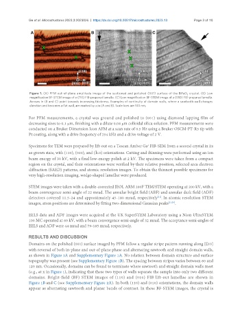
Figure 1. (A) PFM out-of-plane amplitude image of the sectioned and polished (001) surface of the BiFeO crystal. (B) Low
3
magnification BF-STEM image of a (110) FIB-prepared lamella. (C) Low magnification BF-STEM image of a (010) FIB-prepared lamella.
Arrows in (B and C) point towards increasing thickness. Examples of continuity of domain walls, where a sawtooth wall changes
direction and becomes a flat wall, are marked by x in (A and B). Scale bars are 100 nm.
For PFM measurements, a crystal was ground and polished to (001) using diamond lapping film of
decreasing sizes to 0.1 µm, finishing with a dilute 0.04 µm colloidal silica solution. PFM measurements were
conducted on a Bruker Dimension Icon AFM at a scan rate of 0.5 Hz using a Bruker OSCM-PT-R3 tip with
Pt coating, along with a drive frequency of 254 kHz and a drive voltage of 2 V.
Specimens for TEM were prepared by lift-out on a Tescan Amber Ga FIB-SEM from a second crystal in its
+
as-grown state, with (110), (010), and ( 10) orientations. Cutting and thinning were performed using an ion
beam energy of 30 kV, with a final low-energy polish at 2 kV. The specimens were taken from a compact
region on the crystal, and their orientations were verified by their relative position, selected area electron
diffraction (SAED) patterns, and atomic resolution images. To obtain the thinnest possible specimens for
very high-resolution imaging, wedge-shaped lamellae were produced.
STEM images were taken with a double-corrected JEOL ARM 200F TEM/STEM operating at 200 kV, with a
beam convergence semi-angle of 22 mrad. The annular bright field (ABF) and annular dark field (ADF)
detectors covered 11.5-24 and approximately 45-180 mrad, respectively . In atomic resolution STEM
[11]
images, atom positions are determined by fitting two-dimensional Gaussian peaks [11,20] .
EELS data and ADF images were acquired at the UK SuperSTEM Laboratory using a Nion UltraSTEM
100 MC operated at 60 kV, with a beam convergence semi-angle of 32 mrad. The acceptance semi-angles of
EELS and ADF were 44 mrad and 79-185 mrad, respectively.
RESULTS AND DISCUSSION
Domains on the polished (001) surface imaged by PFM follow a regular stripe pattern running along [ 10]
with reversal of both in-plane and out-of-plane phase and alternating sawtooth and straight domain walls,
as shown in Figure 1A and Supplementary Figure 1A. No relation between domain structure and surface
topography was present (see Supplementary Figure 1B). The spacing between stripes varies between 60 and
120 nm. Occasionally, domains can be found to terminate where sawtooth and straight domain walls meet
(e.g., at x in Figure 1), indicating that these two types of walls separate the sample into only two different
domains. Bright-field (BF) STEM images of (110) and (010) FIB lift-out lamellae are shown in
Figure 1B and C (see Supplementary Figure 2A). In both (110) and (010) orientations, the domain walls
appear as alternating sawtooth and planar bands of contrast. In these BF-STEM images, the crystal is