
Page 54 - Read Online
P. 54
Yang et al. Microstructures 2023;3:2023005 https://dx.doi.org/10.20517/microstructures.2022.24 Page 5 of 10
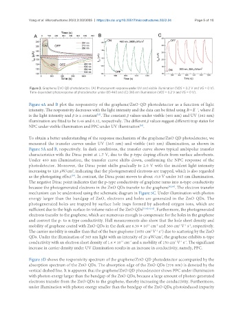
Figure 3. Graphene/ZnO QD photodetector. (A) Photocurrent response under UV and visible illumination (VDS = 0.2 V and VG = 0 V).
Time-dependent photoresponse of photodetector under (B) 460 and (C) 365 nm illumination (VDS = 0.2 V and VG = 0 V).
Figure 4A and B plot the responsivity of the graphene/ZnO QD photodetector as a function of light
intensity. The responsivity decreases with the light intensity and the data can be fitted using R∝E , where E
-1
is the light intensity and β is a constant . The constant β values under visible (460 nm) and UV (365 nm)
[25]
illumination are fitted to be 0.46 and 0.12, respectively. The different β values suggest different trap states for
[59]
NPC under visible illumination and PPC under UV illumination .
To obtain a better understanding of the response mechanism of the graphene/ZnO QD photodetector, we
measured the transfer curves under UV (365 nm) and visible (460 nm) illumination, as shown in
Figure 5A and B, respectively. In dark conditions, the transfer curve shows typical ambipolar transfer
characteristics with the Dirac point at 1.7 V, due to the p-type doping effects from surface adsorbents.
Under 460 nm illumination, the transfer curve shifts down, confirming the NPC response of the
photodetector. Moreover, the Dirac point shifts gradually to 2.0 V with the incident light intensity
2
increasing to 128 μW/cm , indicating that the photogenerated electrons are trapped, which is also regarded
[59]
as the photogating effect . In contrast, the Dirac point moves to about -0.9 V under 365 nm illumination.
The negative Dirac point indicates that the p-type conductivity of graphene turns into n-type conductivity
because the photogenerated electrons in the ZnO QDs transfer to the graphene [42,60] . The electron transfer
mechanism can be understood using the schematic diagram in Figure 5C. Under illumination with photon
energy larger than the bandgap of ZnO, electrons and holes are generated in the ZnO QDs. The
photogenerated holes are trapped by surface hole traps formed by adsorbed oxygen ions, which are
sufficient due to the high surface-to-volume ratio of the ZnO QDs [15,42,61,62] . Furthermore, the photogenerated
electrons transfer to the graphene, which are numerous enough to compensate for the holes in the graphene
and convert the p- to n-type conductivity. Hall measurements also show that the hole sheet density and
-1 -1
mobility of graphene coated with ZnO QDs in the dark are 6.39 × 10 cm and 360 cm V s , respectively.
12
-2
2
The carrier mobility is smaller than that of the bare graphene (1050 cm V s ) due to scattering by the ZnO
-1 -1
2
QDs. Under the illumination of 365 nm light with an intensity of 20 μW/cm , the graphene exhibits n-type
2
-1 -1
2
conductivity with an electron sheet density of 1.6 × 10 cm and a mobility of 150 cm V s . The significant
13
-2
increase in carrier density under UV illumination results in an increase in conductivity, namely, PPC.
Figure 5D shows the responsivity spectrum of the graphene/ZnO QD photodetector accompanied by the
absorption spectrum of the ZnO QDs. The absorption edge of the ZnO QDs (376 nm) is denoted by the
vertical dashed line. It is apparent that the graphene/ZnO QD photodetector shows PPC under illumination
with photon energy larger than the bandgap of the ZnO QDs, because a large amount of photon-generated
electrons transfer from the ZnO QDs to the graphene, thereby increasing the conductivity. Furthermore,
under illumination with photon energy smaller than the bandgap of the ZnO QDs, photoinduced impurity