
Page 53 - Read Online
P. 53
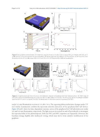
Page 4 of 10         Yang et al. Microstructures 2023;3:2023005  https://dx.doi.org/10.20517/microstructures.2022.24


                Figure 1. Bare graphene photodetector. (A) Schematic diagram of device structure (device area is 100 µm in length and 1200 µm in
                width defined as the area between the two electrodes). (B) Raman spectrum of graphene. (C) Photoelectric on/off response under
                illumination in the UV to visible range (VDS = 0.2 V and VG = 0 V). (D) Responsivity at different wavelengths.


                Figure 2. Graphene/ZnO QD heterostructure. (A) Schematic diagram of graphene/ZnO QD heterostructure. (B) TEM image of
                ZnO QDs. Inset shows HRTEM image of a single ZnO QD. (C) XRD pattern of ZnO QDs. (D) XPS survey spectrum and high-resolution
                spectra of (E) O 1s and (F) Zn 2p for ZnO QDs. (G) Raman and (H) absorption spectra of graphene/ZnO QDs.

               under 313 nm illumination recovers to 4% after 700 s. The opposing photoconductance changes under UV
               and visible illumination confirm the spectrum-selective detection of the graphene/ZnO QD device.
               Figure 3B and C show the time-dependent response curves of the graphene/ZnO QD photodetector under
               365 and 460 nm illumination, respectively. The light sources are turned on and off periodically to investigate
               the reproducibility of the photoresponse. Both the PPC and NPC responses are repeatable. However, the
               baselines change slightly after multicycle testing, which may derive from catalytic modification of the
               graphene.