


Page 74 - Read Online
P. 74
Page 6 of 22                                                          Na et al. Soft Sci. 2026, 6, 25


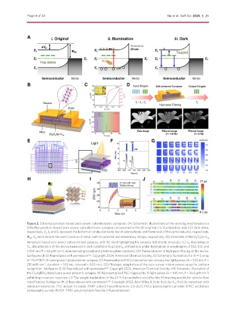
               Figure 2. Schottky junction-based zero-power optoelectronic synapses. (A) Schematic illustrations of the working mechanism in a
               Schottky junction-based zero-power optoelectronic synapse correspond to the (i) original, (ii) illumination, and (iii) dark state,
               respectively. E c , E v  and E F  represent the bottom of conduction band, top of valence band, and Fermi level of the semiconductor, respectively.
               Φ B0 , V bi  and e denote the work function of metal, built-in potential and elementary charge, respectively; (B) Schematic of the Bi 2 O 2 Se-V Se
               nanosheet-based zero-power optoelectronic synapse, with the inset highlighting the vacancy-rich atomic structure; (C) I DS  depending on
               V DS  characteristics of the device measured in dark conditions (top) and I DS  without bias under illumination at wavelengths of 350, 532, and
               1,050 nm (P = 66 μW·cm ), demonstrating broadband photoreception (bottom); (D) Demonstration of high-pass filtering of the device.
                                -2
               Subfigures (B-D) Reproduced with permission [32] . Copyright 2024, American Chemical Society; (E) Schematic illustration of a 10 × 5 array
               of ITO/P3HT/Al zero-power optoelectronic synapse; (F) Representative PSCs induced by two consecutive light pulses (λ = 520 nm, P =
               215 mW·cm , duration = 100 ms, interval = 500 ms); (G) Photopic adaptation of the zero-power vision sensor array for pattern
                       -2
               recognition. Subfigures (E-G) Reproduced with permission [33] . Copyright 2025, American Chemical Society; (H) Schematic illustration of
               the Cs 2 AgBiBr 6 -based zero-power photonic synapse; (I) Representative EPSC triggered by 10 light pulses (λ = 445 nm, P = 36.6 μW·cm )
                                                                                                         -2
               exhibiting in-sensor reservoir; (J) The weight modulation in the 25 × 4 array before and after the 50 training epochs for vehicle-flow
               classification. Subfigures (H-J) Reproduced with permission [34] . Copyright 2022, John Wiley & Sons. Bi 2 O 2 Se-V Se : Bi 2 O 2 Se nanosheet with
               selenium vacancies; ITO: indium tin oxide; P3HT: poly(3-hexylthiophene-2,5-diyl); PSCs: postsynaptic currents; EPSC: excitatory
               postsynaptic current; P(VDF-TrFE): poly(vinylidene fluoride-trifluoroethylene).

