
Page 70 - Read Online
P. 70
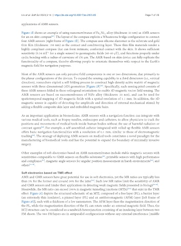
Lin et al. Soft Sci 2023;3:14  https://dx.doi.org/10.20517/ss.2023.05            Page 7 of 25

               applications of AMR sensors.


               Figure 2E shows an example of using nanomembranes of Fe Ni  alloy (thickness: 50 nm) as AMR sensors
                                                                  81
                                                                      19
                                   [41]
               for an on-skin compass . The layout of the compass exploits a Wheatstone bridge configuration to connect
               four AMR sensors [right frame of Figure 2E]. The compass uses silicone elastomer as the substrate and gold
               thin film (thickness: 100 nm) as the contact and conditioning layer. These thin film materials render a
               highly compliant compass that can form intimate, conformal contact with the skin. It shows sufficient
               sensitivity (0.54 mT  for a single sensor) to geomagnetic fields (40-60 μT), and functions properly under
                                -1
               cyclic bending with a radius of curvature of 150 μm. The AMR-based on-skin device can fully replicate the
               functionality of a compass, thereby allowing people to orientate themselves with respect to the Earth’s
               magnetic field for navigation purposes.


               Most of the AMR sensors can only perceive field components in one or two dimensions, due primarily to
               the planar configurations of the devices. To expand the sensing capability to a third dimension (i.e., vertical
               direction), researchers exploit a self-folding process to construct high-density active matrix of magnetic
               sensors with three-dimensional (3D) geometries [Figure 2F] . Specifically, each sensing pixel consists of
                                                                   [87]
               three AMR sensors folded in three orthogonal orientations to enable 3D magnetic vector field sensing. The
               AMR sensors are based on nanomembranes of NiFe alloy (thickness: 20 nm), and can be used for
               spatiotemporal mapping of 3D magnetic fields with a spatial resolution of 1.1 mm. In addition, the 3D
               magnetic sensor is capable of detecting the amplitude and direction of external mechanical stimuli by
               adding a flexible composite skin layer and embedded magnetic hairs.


               As an important application in biomedicine, AMR sensors with a navigation function can integrate with
               various medical tools, such as biopsy needles, endoscopes and catheters, to allow physicians to track the
               positions and movements of medical tools inside human bodies without the use of harmful radiation or
               contrast agents . For example, a self-assembled catheter integrated with rolled-up flexible AMR sensors
                            [88]
               offers basic navigation functionalities with a resolution of 0.1 mm, similar to those of electromagnetic
               tracking . The strategy of deploying AMR sensors on medical tools constitutes a novel paradigm for the
                      [89]
               manufacturing of biomedical tools and has the potential to expand the boundary of minimally invasive
               surgery.


               Other examples of soft electronics based on AMR nanomembranes include stable magnetic sensors with
               sensitivities comparable to GMR sensors on flexible substrates , printable sensors with high performance
                                                                    [90]
               and compliance , magnetic angle sensors for angular position measurement in harsh environments , and
                             [91]
                                                                                                    [92]
               others [93-95] .
               Soft electronics based on TMR effect
               AMR and GMR sensors have great potential for use in soft electronics, yet the MR ratios are typically less
               than 5% for the former and around 50% for the latter . Such low MR ratios limit the sensitivity of AMR
                                                             [96]
               and GMR sensors and hinder their applications in detecting weak magnetic fields presented in biology [97-99] .
               Meanwhile, the MR ratio can exceed 200% in magnetic tunneling junctions (MTJs)  that exist in the TMR
                                                                                     [100]
               effect. Figure 2G depicts the structural schematic of an MTJ, composed of a free layer (FL), a barrier layer
               (an extremely thin insulator), a pinned layer (PL) and an antiferromagnetic (AFM) layer [left frame of
               Figure 2G], each with a thickness of a few nanometers. The AFM layer fixes the magnetization direction of
               the PL, while the magnetization direction of the FL can rotate under an external magnetic field. Thus, the
               MTJ structure can be considered as a sandwich heterojunction consisting of an insulating layer between two
               FM sheets. The two FM layers are in antiparallel configurations without any external interference [middle