
Page 241 - Read Online
P. 241
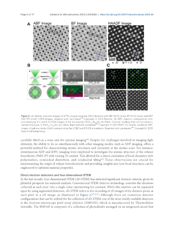
Page 6 of 17        Cabral et al. Microstructures 2023;3:2023040  https://dx.doi.org/10.20517/microstructures.2023.39


                Figure 3. (A) Atomic resolution images of SrTiO  viewed along the [001] direction with ABF (11-22 mrad), BF (0-22 mrad), and ADF
                                                3
                (90-170 mrad) STEM images. Adapted with  permission [33] . Copyright © 2012 Elsevier. (B) DPC detector configuration with
                accompanying A-C and B-D STEM images of the ferroelectric Pb(Zr Ti )O  thin films. Contrast resulting from the ferroelectric
                                                               0.2  0.8  3
                domain structures in Pb(Zr Ti )O  are visible. Reprinted with permission [34]  Copyright © 2021 MDPI. (C) Atomic resolution iDPC
                                  0.2  0.8  3
                images of gallium nitride (GaN) oriented along the [11 0] and [10 1] orientations. Reprinted with  permission [35] . Copyright © 2018
                Nature Publishing Group.
                                                            [20]
               carefully tilted on a zone axis for optimal imaging . Despite the challenges involved in imaging light
               elements, the ability to do so simultaneously with other imaging modes, such as ADF imaging, offers a
               powerful method for characterizing atomic structures and chemistry at the atomic scale. For instance,
               simultaneous ADF and iDPC imaging were employed to investigate the atomic structure of the relaxor
               ferroelectric PMN-PT with varying Ti content. This allowed for a direct correlation of local chemistry with
               polarization,  octahedral  distortion,  and  octahedral  tilting . These  observations  are  crucial  for
                                                                      [40]
               understanding the origin of relaxor ferroelectricity and providing insights into how local structures can be
               engineered to optimize material properties.

               Direct electron detectors and four-dimensional STEM
               In the last decade, four-dimensional STEM (4D-STEM) has attracted significant research interest, given its
               plentiful prospects for material analysis. Conventional STEM detector technology converts the electrons
               collected at each pixel into a single value representing the contrast. While this number can be expanded
               upon by using segmented detectors, 4D-STEM refers to the recording of 2D images of the electron probe at
               each pixel in a 2D image, as illustrated in Figure 1C [19,41,42] . Although there are numerous detector
               configurations that can be utilized for the collection of 4D-STEM, one of the most widely available detectors
               is the electron microscope pixel array detector (EMPAD), which is manufactured by Thermofisher
               Scientific. The EMPAD is composed of a collection of photodiodes arranged on an integrated circuit that