
Page 240 - Read Online
P. 240
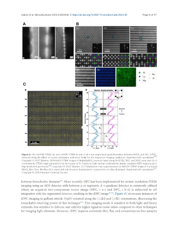
Cabral et al. Microstructures 2023;3:2023040  https://dx.doi.org/10.20517/microstructures.2023.39  Page 5 of 17


                Figure 2. (A) HAADF-STEM (a) and LAADF-STEM (b and c) of a low-angle twist grain boundary between SrTiO  and Nb:  SrTiO ,
                                                                                              3          3
                                                                                                        [25]
                demonstrating the effect of crystal orientation and strain fields for the respective imaging conditions. Reprinted with  permission  .
                Copyright © 2007 Elsevier. (B) HAADF-STEM images of NaLaMgWO  ceramics taken along the [111], [110], and [100] zone axes (a-c)
                                                              6
                confirmed by STEM image simulations for each zone (d-f). Chemical order further confirmed by atomic resolution EDS mapping (g-i).
                                  [26]
                Reprinted with  permission  . Copyright © 2022 Elsevier. (C) Polarization map superimposed on HAADF-STEM image of Ca-doped
                                                                                                        [27]
                BiFeO  thin films. Profiles of in-plane and out-of-plane displacement components are also displayed. Reprinted with  permission  .
                    3
                Copyright © 2018 American Chemical Society.
               between ferroelectric domains . More recently, DPC has been implemented for atomic resolution STEM
                                         [34]
               imaging using an ADF detector with between 2-16 segments. A 4-quadrant detector is commonly utilized
               where an acquired two-component vector image (DPC  = a-c and DPC  = b-d) is subjected to 2D
                                                                  x
                                                                                 y
               integration with the segmented detector, resulting in the iDPC image [35,39] . Figure 3C showcases instances of
               iDPC imaging in gallium nitride (GaN) oriented along the [11 0] and [10 1] orientations, illustrating the
               remarkable resolving power of this technique . This imaging mode is sensitive to both light and heavy
                                                       [35]
               elements, less sensitive to defocus, and exhibits higher signal-to-noise ratios compared to other techniques
               for imaging light elements. However, iDPC requires extremely thin, flat, and contamination-free samples