
Page 16 - Read Online
P. 16
Feng et al. Microstructures 2023;3:2023017 https://dx.doi.org/10.20517/microstructures.2023.01 Page 3 of 7
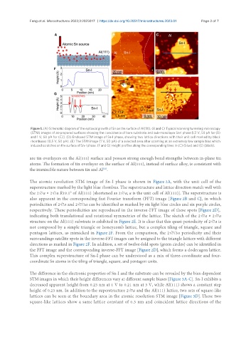
Figure 1. (A) Schematic diagram of the epitaxial growth of Sn on the surface of Al(111). (B and C) Typical scanning tunneling microscopy
(STM) images of as-prepared surfaces showing the coexistence of bare substrate and sub-monolayer Sn-I phase [(2 V, 50 pA for (B)
and 1 V, 50 pA for (C)]. (D) Enclosed STM image of Sn-I phase, showing two lattice directions with their unit cell marked by black
rhombuses (0.5 V, 50 pA). (E) The STM image (1 V, 50 pA) of a selected area after scanning at an extremely low sample bias which
induced scratches on the surface of Sn-I phase. (F and G) Height profiles along the corresponding lines in (C) (blue) and (E) (black).
are tin overlayers on the Al(111) surface and possess strong enough bond strengths between in-plane tin
atoms. The formation of tin overlayer on the surface of Al(111), instead of surface alloy, is consistent with
the immiscible nature between tin and Al .
[22]
The atomic resolution STM image of Sn-I phase is shown in Figure 2A, with the unit cell of the
superstructure marked by the light blue rhombus. The superstructure and lattice direction match well with
the 2√7a × 2√7a R19.1° of Al(111) [shortened as 2√7a, a is the unit cell of Al(111)]. The superstructure is
also apparent in the corresponding fast Fourier transform (FFT) image [Figure 2B and C], in which
periodicities of 2√7a and 2√7/3a can be identified as marked by six light blue circles and six purple circles,
respectively. These periodicities are reproduced in the inverse-FFT image of these spots [Figure 2D],
indicating both translational and rotational symmetries of the lattice. The sketch of the 2√7a × 2√7a
structure on the Al(111) substrate is exhibited in Figure 2E. It is clear that this quasi-periodicity of 2√7a is
not composed by a simple triangle or honeycomb lattice, but a complex tiling of triangle, square and
pentagon lattices, as mimicked in Figure 2F. From the comparison, the 2√7/3a periodicity and their
surroundings satellite spots in the inverse-FFT images can be assigned to the triangle lattices with different
directions as marked in Figure 2F. In addition, a set of twelve-fold spots (green circles) can be identified in
the FFT image and the corresponding inverse-FFT image [Figure 2D], which forms a dodecagon lattice.
This complex superstructure of Sn-I phase can be understood as a mix of three-coordinate and four-
coordinate Sn atoms in the tiling of triangle, square, and pentagon units.
The difference in the electronic properties of Sn-I and the substrate can be revealed by the bias-dependent
STM images in which their height differences vary at different sample biases [Figure 3A-C]. Sn-I exhibits a
decreased apparent height from 0.23 nm at 1 V to 0.21 nm at 3 V, while Al(111) shows a constant step
height of 0.23 nm. In addition to the superstructure 2√7a and the Al(111) lattice, two sets of square-like
lattices can be seen at the boundary area in the atomic resolution STM image [Figure 3D]. These two
square-like lattices show a same lattice constant of 0.3 nm and coincident lattice directions of the