
Page 17 - Read Online
P. 17
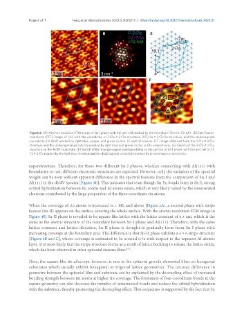
Page 4 of 7          Feng et al. Microstructures 2023;3:2023017  https://dx.doi.org/10.20517/microstructures.2023.01


                Figure 2. (A) Atomic resolution STM image of Sn-I phase with the unit cell marked by the rhombus (-50 mV, 50 pA). (B) Fast Fourier
                transform (FFT) image of (A) with the periodicity of 2√7a × 2√7a structure, 2√7/3a × 2√7/3a structure, and the dodecagonal
                periodicity (12-fold) marked by light blue, purple, and green circles. (C and D) Inverse-FFT image obtained from the 2√7a × 2√7a
                structure and the dodecagonal periodicity marked by light blue and green circles in (B), respectively. (E) Sketch of the 2√7a × 2√7a
                structure on the Al(111) substrate. (F) Sketch of the triangle-square-pentagon tiling on the surface of Sn-I phase, with the unit cell of 2√
                7a × 2√7a marked by the light blue rhombus and the dodecagonal periodicity marked by green shapes, respectively.


               superstructure. Therefore, for these two different Sn-I phases, whether connecting with Al(111) with
               boundaries or not, different electronic structures are expected. However, only the variation of the spectral
               weight can be seen without apparent difference in the spectral features from the comparison of Sn-I and
               Al(111) in the dI/dV spectra [Figure 3E]. This indicates that even though Sn-Sn bonds form in Sn-I, strong
               orbital hybridization between tin atoms and Al atoms exists, which is very likely raised by the unsaturated
               electrons contributed by the large proportion of the three-coordinate tin atoms.


               When the coverage of tin atoms is increased to 1 ML and above [Figure 4A], a second phase with stripe
               feature (Sn-II) appears on the surface covering the whole surface. With the atomic resolution STM image in
               Figure 4B, Sn-II phase is revealed to be square-like lattice with the lattice constant of 0.3 nm, which is the
               same as the atomic structure of the boundary between Sn-I phase and Al(111). Therefore, with the same
               lattice constant and lattice direction, Sn-II phase is thought to gradually form from Sn-I phase with
               increasing coverage at the boundary area. The difference is that Sn-II phase exhibits a 4 × 6 stripe structure
               [Figure 4B and C], whose coverage is estimated to be around 0.78 with respect to the topmost Al atomic
               layer. It is most likely that the stripe structure forms as a result of lattice buckling to release the lattice strain,
               which has been observed in other epitaxial stanene films .
                                                              [5-7]
               Here, the square-like tin allotrope, however, is rare in the epitaxial growth elemental films on hexagonal
               substrates which usually exhibit hexagonal or trigonal lattice geometries. The unusual difference in
               geometry between the epitaxial film and substrate can be explained by the decoupling effect of increased
               bonding strength between tin atoms at higher tin coverage. The formation of four-coordinate bonds in the
               square geometry can also decrease the number of unsaturated bonds and reduce the orbital hybridization
               with the substrate, thereby promoting the decoupling effect. This conjecture is supported by the fact that Sn