
Page 18 - Read Online
P. 18
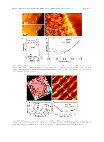
Feng et al. Microstructures 2023;3:2023017  https://dx.doi.org/10.20517/microstructures.2023.01  Page 5 of 7


                Figure 3. (A and B) STM images of a selected area with coexistence of Sn-I phase and bare substrate under different sample biases [3
                V for (A) and 1 V for (B)]. (C) Height profiles along the corresponding lines in (A) (red curve) and (B) (blue curve). (D) The STM image
                of a boundary area between Sn-I phase and the bare substrate showing the square-like lattice at the boundary (-50 mV, 50 pA). (E)
                dI/dV spectra on Al(111) and Sn-I phase.


                Figure 4. (A) STM image of the surface after deposition of > 1 ML Sn on Al(111) showing stripe structure (Sn-II phase) and abundant
                clusters on the surface (2.5 V, 50 pA, image size is 50 nm × 50 nm). (B) Atomic resolution STM image of Sn-II phase (16 mV, 900 pA).
                (C) Height profile along the white line in (B). (D) dI/dV spectra on the hill and valley of the stripe structure of Sn-II phase.