
Page 19 - Read Online
P. 19
Page 4 of 12 Zhang et al. Microstructures 2023;3:2023010 https://dx.doi.org/10.20517/microstructures.2022.39
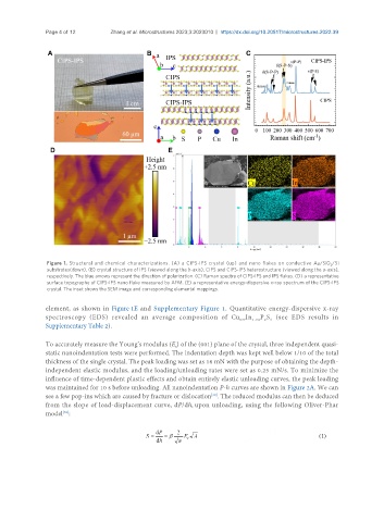
Figure 1. Structural and chemical characterizations. (A) a CIPS-IPS crystal (up) and nano flakes on conductive Au/SiO /Si
2
substrates(down). (B) crystal structure of IPS (viewed along the b-axis), CIPS and CIPS-IPS heterostructure (viewed along the a-axis),
respectively. The blue arrows represent the direction of polarization. (C) Raman spectra of CIPS-IPS and IPS flakes. (D) a representative
surface topography of CIPS-IPS nano flake measured by AFM. (E) a representative energy-dispersive x-ray spectrum of the CIPS-IPS
crystal. The inset shows the SEM image and corresponding elemental mappings.
element, as shown in Figure 1E and Supplementary Figure 1. Quantitative energy-dispersive x-ray
spectroscopy (EDS) revealed an average composition of Cu In 1.04 P S (see EDS results in
2 6
0.57
Supplementary Table 2).
To accurately measure the Young’s modulus (E ) of the (001) plane of the crystal, three independent quasi-
s
static nanoindentation tests were performed. The indentation depth was kept well below 1/10 of the total
thickness of the single crystal. The peak loading was set as 16 mN with the purpose of obtaining the depth-
independent elastic modulus, and the loading/unloading rates were set as 0.25 mN/s. To minimize the
influence of time-dependent plastic effects and obtain entirely elastic unloading curves, the peak loading
was maintained for 10 s before unloading. All nanoindentation P-h curves are shown in Figure 2A. We can
[38]
see a few pop-ins which are caused by fracture or dislocation . The reduced modulus can then be deduced
from the slope of load-displacement curve, dP/dh, upon unloading, using the following Oliver-Phar
model :
[39]