


Page 49 - Read Online
P. 49
Zhang et al. Soft Sci. 2026, 6, 16                                                Page 7 of 17


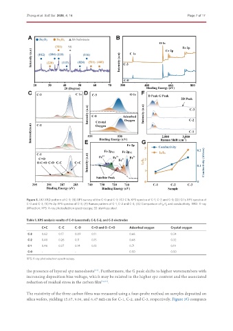
               Figure 3. (A) XRD pattern of C-3; (B) XPS survey of the C-0 and C-3; (C) C 1s XPS spectra of C-1, C-2 and C-3; (D) O 1s XPS spectra of
               C-0 and C-3; (E) Fe 2p XPS spectra of C-3; (F) Raman pattern of C-1, C-2 and C-3; (G) Comparison of I D /I G  and conductivity. XRD: X-ray
               diffraction; XPS: X-ray photoelectron spectroscopy; SS: stainless steel.

               Table 1. XPS analysis results of C-0 (uncoated), C-1, C-2, and C-3 electrodes

                      C=C      C–C     C–O      C=O and O–C=O      Adsorbed oxygen      Crystal oxygen
               C-3    0.63     0.17    0.09     0.11               0.66                 0.34
               C-2    0.48     0.26    0.11     0.15               0.68                 0.32
               C-1    0.46     0.27    0.14     0.13               0.71                 0.19
               C-0    -        -       -                           0.50                 0.50

               XPS: X-ray photoelectron spectroscopy.

               the presence of layered sp2 nanosheets . Furthermore, the G peak shifts to higher wavenumbers with
                                                 [31]
               increasing deposition bias voltage, which may be related to the higher sp2 content and the associated
               reduction of residual stress in the carbon film [32,33] .

               The resistivity of the three carbon films was measured using a four-probe method on samples deposited on
               silica wafers, yielding 15.67, 9.06, and 6.47 mΩ·cm for C-1, C-2, and C-3, respectively. Figure 3G compares

