


Page 47 - Read Online
P. 47
Zhang et al. Soft Sci. 2026, 6, 16                                                Page 5 of 17


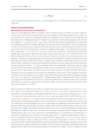
                                                           3600 ×
                                                          =                                             (3)

               where I represents the discharge current, t is the discharge time, ΔV is the potential window, and S is the
               active area.


               RESULTS AND DISCUSSION
               Morphological and structural characterization
               Figure 2A and B illustrates SEM micrographs of the SS substrate before and after the anodic oxidation
               process. The initially smooth SS surface became porous, with pore radii of approximately 40 nm, which can
               be attributed to the steady-state competition between the oxidation of Fe, Cr, and Ni in the SS substrate and
               the etching of the resulting metal oxides . Figure 2C-E presents the carbon film deposition result with the
                                                 [20]
               bias voltage of -5, +20 and +100 V for 10 min, respectively. The entire surface and sidewalls were coated with
               one homogeneous film successfully, making the pores much narrower than before. Since the nanoporous
               structure was neither perfectly tubular nor flat on the top surface, the coated film appeared as particles with
               sizes on the order of tens of nanometers. As shown in Supplementary Figure 1, the thicknesses of the carbon
               films coated under -5, +20, and +100 V were 60, 45, and 40 nm, respectively, consistent with the observed
               morphology of the samples. Supplementary Figure 2 presents the surface of +100 V-coated electrodes with
               different deposition times. It can be clearly observed that the sidewalls of the nanoporous structure
               thickened, and when the deposition time exceeded 20 min, the top surface was fully covered by the carbon
               film. Figure 2F shows the TEM result of the C-3 sample, where a tubular structure with a radius of 38 nm is
               clearly visible. A dark layer attached to the sidewall of the tubular structure, which was not observed in our
               previous anodized SS reports [5,11-12] , can be considered as the coated carbon film. In the high-resolution image
               in Figure 2G, the major lattice spacings of 0.250 and 0.369 nm can be indexed to the (110) and (012) crystal
               planes of Fe O , respectively. Several bowed and discontinuous lattices are observed in the dark region,
                         2
                            3
               interpreted as stacks of graphene sheets within the amorphous carbon matrix. These graphene sheets may
               contribute to the decreased electrical resistance of the carbon film and become visible at irradiation energies
               above 40 eV, as reported by Wang and Diao . Supplementary Figure 3 displays the EDS spectrum of the
                                                     [16]
               C-3 sample, where the elements Fe, Ni, Mn, Cr, and O are attributed to the oxidized SS foil, and C originates
               from both the carbon film coating and the SS substrate. Figure 2H-K shows the uniform distribution of the
               three major elements: C, O, and Fe.

               Figure 3A shows the XRD spectrum of the C-3 sample. The characteristic peaks at 24.3°, 33.4°, 36.0°, 41.3°,
               50.0°, and 54.6° are attributed to the (012), (104), (110), (113), (024), and (116) planes of Fe O  (Joint
                                                                                                    3
                                                                                                  2
               Committee on Powder Diffraction Standards, JCPDS No. 84-0311), respectively. The peaks at 30.0°, 35.3°,
               57.2°, and 62.8° correspond to the (220), (311), (511), and (440) planes of Fe O  (JCPDS No.88-0351),
                                                                                    3
                                                                                      4
               respectively. The peak at 44.3° is assigned to the unevenly distributed martensite within the SS foils . No
                                                                                                     [21]
               obvious peak corresponding to graphitic carbon was observed in the spectrum, which can be attributed to
               the relatively low content of graphene sheets in the carbon film, as confirmed by TEM observations. The XPS
               spectra of the fabricated electrodes are shown in Figure 3B-E. Consistent with the EDS results, the survey
               spectrum of C-3 [Figure 3B] clearly confirms the presence of C, O, Cr, and Fe, indicating successful carbon
               film deposition. Figure 3C shows the C 1s peak, which can be deconvoluted into four Gaussian components
               at approximately 284.6, 285.2, 286.6, and 288.8 eV, corresponding to C=C (sp2 phase), C–C (sp3 phase), C–O
               bonds, and a combination of C=O and O–C=O bonds, respectively [22,23] . From the analytical data in Table 1, it
               can be concluded that with the increase of deposition bias voltage from -5 to +100 V, the sp2 content
               increased, leading to higher conductivity of the C-3 electrode compared to C-2 and C-1. This result is
               consistent with the work by Wang and Diao and can be explained by the damage to graphene sheets in the
               carbon film under negative substrate bias voltage and the structural transition from amorphous carbon to
               graphene sheets under electron irradiation at positive substrate bias voltage . The O 1s peaks of C-0 and
                                                                                [16]

