
Page 73 - Read Online
P. 73
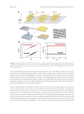
Page 6 of 9                                Wang. Soft Sci 2024;4:25  https://dx.doi.org/10.20517/ss.2024.14


                Figure 2. (A) Schematic illustration of the P3HT polymer chain orientation and the process of aligning the polymer chain to chain-on
                orientation. The scale bar denotes 10 µm; (B) The current-voltage characteristics and the extracted charge carrier mobility of the
                aligned P3HT in comparison to conventional smooth film. Images reproduced with permission [28] . Copyright 2016, Wiley-VCH. P3HT:
                Poly(3-hexylthiophene).


                                                                    [8]
               due to the thermal interaction between nearby Peltier elements . The trade-off between the ΔT and ΔQ can,
               nevertheless, be avoided using cascade Peltier modules where multiple stages of Peltier elements are stacked
               together with the thin device with high ΔQ in contact with the heat reservoir and thicker devices stacked on
               top of the thinner device to enable higher ΔT. In terms of the fabrication technology for such cascade Peltier
               devices with organic semiconductors, inkjet printing or electrohydrodynamic printing would be a suitable
               preparation technique as these deposition methods waste minimal material and could control the thickness
               precisely by adjusting the number of printing passes .
                                                           [12]
               Another important aspect to consider for organic Peltier cooling devices is contact resistance. Two types of
               contact resistance exist: the electrical contact resistance between the electrode and organic semiconductor
               interface and the thermal contact resistance that can either be internal (between the electrode and organic
               semiconductor) or external (between the Peltier cooling device and the heat source). The interfacial
               electrical contact resistance would need to be minimized to avoid additional Joule heating in the device. The
               electrical contact resistance could be reduced by contact doping and the selection of electrode material with
               work function aligning with the energy level of the organic semiconductors where a lot of work has been
               done in the organic transistor technology . As for thermal contact resistance, the ideal internal thermal
                                                   [35]