
Page 160 - Read Online
P. 160
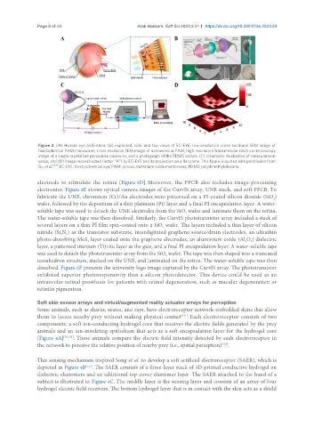
Page 8 of 33                          Arab Hassani. Soft Sci 2023;3:31  https://dx.doi.org/10.20517/ss.2023.23


                Figure 2. (A) Human eye and retina; (B) exploded, side, and top views of EC-EYE; low-resolution cross-sectional SEM image of
                hemispherical PAM/nanowires; cross-sectional SEM image of nanowires in PAM; high-resolution transmission electron microscopy
                image of a single-crystalline perovskite nanowire; and a photograph of the PDMS socket; (C) schematic illustration of measurement
                setup; and (D) image reconstructed (letter “A”) by EC-EYE and its projection on a flat plane. This figure is quoted with permission from
                Gu et al. [27] . EC-EYE: Electrochemical eye; PAM: porous aluminium oxide membranes; PDMS: polydimethylsiloxane.

               electrode to stimulate the retina [Figure 3D]. Moreover, the FPCB also includes image-processing
               electronics. Figure 3E shows optical camera images of the CurvIS array, UNE stack, and soft FPCB. To
               fabricate the UNE, chromium (Cr)/Au electrodes were patterned on a PI-coated silicon dioxide (SiO )
                                                                                                         2
               wafer, followed by the deposition of a thin platinum (Pt) layer and a final PI encapsulation layer. A water-
               soluble tape was used to detach the UNE electrodes from the SiO  wafer and laminate them on the retina.
                                                                       2
               The water-soluble tape was then dissolved. Similarly, the CurvIS phototransistor array included a stack of
               several layers on a thin PI film spin-coated onto a SiO  wafer. The layers included a thin layer of silicon
                                                               2
               nitride (Si N ) as the transistor substrate, interdigitated graphene source/drain electrodes, an ultrathin
                          4
                        3
               photo-absorbing MoS  layer coated onto the graphene electrodes, an aluminium oxide (Al O ) dielectric
                                                                                              2
                                                                                                3
                                  2
               layer, a patterned titanium (Ti)/Au layer as the gate, and a final PI encapsulation layer. A water-soluble tape
               was used to detach the phototransistor array from the SiO  wafer. The tape was then shaped into a truncated
                                                                2
               icosahedron structure, stacked on the UNE, and laminated on the retina. The water-soluble tape was then
               dissolved. Figure 3F presents the university logo image captured by the CurvIS array. The phototransistor
               exhibited superior photoresponsivity than a silicon photodetector. This device could be used as an
               intraocular retinal prosthesis for patients with retinal degeneration, such as macular degeneration or
               retinitis pigmentosa.

               Soft skin sensor arrays and virtual/augmented reality actuator arrays for perception
               Some animals, such as sharks, skates, and rays, have electroreceptor network-embedded skins that allow
               them to locate nearby prey without making physical contact . Each electroreceptor consists of two
                                                                      [131]
               components: a soft ion-conducting hydrogel core that receives the electric fields generated by the prey
               animals and an ion-insulating epithelium that acts as a soft encapsulation layer for the hydrogel core
               [Figure 4A] [53,132] . These animals compare the electric field intensity detected by each electroreceptor in
               the network to perceive the relative position of nearby prey (i.e., spatial perception) .
                                                                                     [132]
               This sensing mechanism inspired Song et al. to develop a soft artificial electroreceptor (SAER), which is
               depicted in Figure 4B . The SAER consists of a three-layer stack of 3D-printed conductive hydrogel on
                                  [117]
               dielectric elastomers and an additional top-cover elastomer layer. The SAER attached to the hand of a
               subject is illustrated in Figure 4C. The middle layer is the sensing layer and consists of an array of four
               hydrogel electric field receivers. The bottom hydrogel layer that is in contact with the skin acts as a shield