


Page 98 - Read Online
P. 98
Page 22 of 31                       Shu et al. J. Mater. Inf. 2025, 5, 36  https://dx.doi.org/10.20517/jmi.2025.13


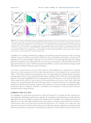
                Figure 11. (A) Schematic representation of organic-inorganic hybrid semiconductors. Hybrid semiconductors can be divided into type I,
                HISSs, and type II, HHSs. Among the HOIPs, 2D Ruddlesden-Popper layered perovskite has common features of type I and II; (B)
                Tetrahedral bonding HHSs investigated are classified as type II. The GaAs-based HHSs in different phases with different numbers of
                inorganic  semiconductor  sublayers  are  shown  as  instances.  Copyright  2022,  American  Chemical  Society,  Reproduced  with
                permission [148] ; (C) The framework for screening DHOIPs by combining ML models and DFT calculations. Copyright 2022, Royal Society
                of Chemistry, Reproduced with  permission [149] . HISSs: Hybrid ion-substituting semiconductors; HHSs: hybrid heterostructure
                semiconductors; HOIPs: hybrid organic-inorganic perovskites; 2D: two-dimensional; DHOIPs: double hybrid organic-inorganic
                perovskites; ML: machine learning; DFT: density functional theory.


               capabilities for searching, downloading, analyzing, and predicting material properties online, providing
               valuable resources for further research into HOIPs and other related fields, particularly in energy and PV
               applications. The model developed a database of 304,920 HOIP structures through this approach, utilizing
               geometric descriptors to precisely predict electronic and structural properties. This innovative data-driven
               approach broadens the scope of HOIP materials and establishes a scalable model for discovering materials
               with enhanced stability and optoelectronic performance.


               To provide a comprehensive overview of the evolution of ML applications in optoelectronic materials
               discovery, we have summarized the ML studies discussed above in chronological order, as presented in
               Table 1. This timeline illustrates the progression from early implementations utilizing simple descriptors
               and regression models to more sophisticated approaches, including CNNs, GNNs, BO, and integrated ML
               pipelines. This progress highlights the increasing sophistication and integration of ML methods in the field,
               which improves the efficiency and accuracy of the material discovery process. Each study collectively
               advances our understanding of ML-driven HT approaches to transform discovery for sustainable, high-
               performance optoelectronic materials. Together, they underscore a cohesive strategy: leveraging predictive
               models and rigorous validation methods to streamline the development of next-generation materials
               essential for future energy solutions.


               SUMMARY AND OUTLOOK
               We highlight the substantial advancements achieved through HT screening and ML techniques in
               discovering and optimizing optoelectronic materials. By integrating computational power with predictive
               algorithms, ML has successfully accelerated the identification of candidates with optimized properties for
               applications in solar cells, light-emitting devices, photocatalytic materials, and photodetectors, marking a
               transformative shift from traditional experimental approaches. HT methods now enable the rapid
               assessment of extensive chemical and structural spaces, allowing systematic exploration of parameters that
               define key optoelectronic properties. In particular, the application of ML models has enhanced predictive

