


Page 87 - Read Online
P. 87
Shu et al. J. Mater. Inf. 2025, 5, 36  https://dx.doi.org/10.20517/jmi.2025.13  Page 11 of 31


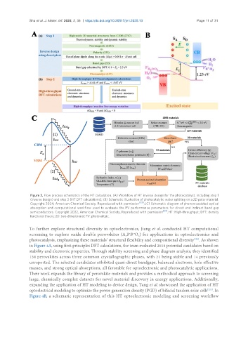
                Figure 3. Flow process schematics of the HT calculation. (A) Workflow of HT inverse design for the photocatalyst, including step 1
                (inverse design) and step 2 (HT DFT calculations); (B) Schematic illustration of photocatalytic water splitting on a 2D polar material.
                Copyright 2024, American Chemical Society, Reproduced with  permission [120] ; (C) Schematic diagram of phonon-assisted optical
                absorption  and  computational  workflow  used  to  evaluate  the  PV  performance  parameters  for  direct  and  indirect  band  gap
                semiconductors. Copyright 2022, American Chemical Society, Reproduced with  permission [121] . HT: High-throughput; DFT: density
                functional theory; 2D: two-dimensional; PV: photovoltaic.


               To further explore structural diversity in optoelectronics, Jiang et al. conducted HT computational
               screening to explore oxide double perovskites (A B′B′′O ) for applications in optoelectronics and
                                                             2
                                                                   6
               photocatalysis, emphasizing these materials’ structural flexibility and compositional diversity . As shown
                                                                                              [122]
               in Figure 4A, using first-principles DFT calculations, the team evaluated 2018 potential candidates based on
               stability and electronic properties. Through stability screening and phase diagram analysis, they identified
               138 perovskites across three common crystallographic phases, with 21 being stable and 14 previously
               unreported. The selected candidates exhibited quasi-direct bandgaps, balanced electrons, hole effective
               masses, and strong optical absorptions, all favorable for optoelectronic and photocatalytic applications.
               Their work expands the library of perovskite materials and provides a methodical approach to screening
               large, chemically complex datasets for novel material discovery in energy applications. Additionally,
               expanding the application of HT modeling to device design, Tang et al. showcased the application of HT
                                                                                                     [123]
               optoelectrical modeling to optimize the power generation density (PGD) of bifacial tandem solar cells . In
               Figure 4B, a schematic representation of this HT optoelectronic modeling and screening workflow

