
Page 49 - Read Online
P. 49
Bai et al. Soft Sci 2023;3:40 https://dx.doi.org/10.20517/ss.2023.38 Page 15 of 34
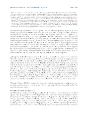
LMNPs are based on the induction of cadmium ions by a three-phase electric field; (ii) LMNPs absorb UV light; (iii) The solid-core
liquid-shell structure of GaNPs senses temperature changes; (B) LMNPs-based one-dimensional circuit structures: (i) Preparation of
conductive pathways from sintered nano-LMs; (ii) High conductivity of nano-LM circuits [174] ; (iii) Nano-LMs for the preparation of
conductive fibres [178] ; (C) Nano-LM planar circuit structure: (i) Multiple ways of preparing plannar structures and sintering; (ii) Self-
sintering of liquid metal to form planar structures; (iii) Stretchability of flat structures [184] ; (iv) Plane structures rich in other sensing
properties [163] ; (D) Nanometer LM embedded elastomer structure: (i) Cross-linking network of LMEE; (ii) LMEE material with good
strain sensitivity; (iii) Multiple interactions give LMEE materials self-adhesive properties [190] ; (iv) The strong self-healing capability of
LMEE; (v) LMEE formed by multiple conductive fillers. CNF: Cellulose nanofiber; CNT: carbon nanotube; LMEE: LM embedded
elastomer; LMNPs: LM nanoparticles; MEK: methyl ethyl ketone; PAA: poly(acrylic acid); PDMS: polydimethylsiloxane; PVDF-HFP-TFE:
poly(vinylidene fluoride-hexafluoropropylene-tetrafluoroethylene); SA: sodium alginate; UV: ultraviolet.
Janus film through a spontaneous density deposition-induced self-assembly process [Figure 5B i] . The
[172]
LMNPs deposited side could be facially activated into conductive paths via simple scratching. This work
exhibited that it is possible to manufacture substrate-ink-integrated materials, which is optimistic for
customized electronics. Similarly, Wu et al. prepared LM-LAPONITE ink to form a layered structure, and
[173]
LMNPs could self-assemble under the effect of capillary force . For healthcare applications, the biosafety
and stability of materials are always of rigorous concern, so encapsulated LMNPs were developed [120,174,175] . Li
et al. demonstrated that this practice was also suitable for LMNPs encapsulated in biocompatible hydrogel
shells and realized conductive traces with the conductivity of ~10 S∙m on multiple substrates, including
-1
5
human skins [Figure 5B ii] . Laser sintering, as a kind of thermal sintering technique, further improves
[174]
6
-1
the conductivity of conductive paths up to 3 × 10 S∙m , which is comparable to the conductivity of bulk
EGaIn [176,177] . These examples verified multiple accesses for LMNPs to coalesce into conductive traces on
multiple substrates with high resolution, lower electrical resistivity, and customized patterns.
Although the displayed conductive paths in this section were actually areas instead of one-dimension
“lines”, the function they realized is simply the one-direction transmission of electrons and guarantees the
most fundamental conduction in their works. Thus, we define such structures as the 1D form here; complex
and more functionalized circuit structures are defined as the 2D form, which will be presented in the next
section. Under this principle, besides activated conductive paths on substrates, LMNPs could also be fused
in sheath-core fibers to work as cables. Zheng et al. applied the coaxial wet spinning method to fabricate a
sheath-core fiber with PVDF-HFP-TFE [poly(vinylidene fluoride-hexafluoropropylene-
tetrafluoroethylene)]/LM particles/MEK (methyl ethyl ketone) as core and PVDF-HFP-TFE/poly(ethylene
glycol) diacrylate/Irgacure 184/MEK as a sheath, which was elastic and characterized as just slightly thicker
[178]
than human hairs [Figure 5B iii] . Ning et al. reported a stretchable fiber composed of dimethyl
formamide/LMNPs/PU as core and dimethyl formamide/PU as sheath . The stable conductivity of such a
[179]
structure was verified in a simple LED circuit under cycled stretching and relaxation state in their works.
The basic 1D form of LMNPs, which resulted in coalesced conductive structures, provided perspective for
[179]
patterning intricate circuits on various substrates or combining LM-based fibers with fabrics to
constitute functional sensors.
Nano-LM planar (2D) circuit structure
In addition to conducting electrical signals, LM materials can also be a source of changes in electrical
signals. Since the generation of electrical signals takes the form of the entire material plane and the
information source is distributed throughout every point on the plane, we define this structure as a planar
[180]
structure. To adjust the adhesion of LM on the surface, surfactants can be used to modify LMNPs . The
resulting LM electronic ink can adhere tightly to objects such as skin and balloons. Zhang et al. achieved
rapid preparation of LM planar structures by preparing a thin layer of LMNPs by spraying . Following a
[181]
similar approach, Li et al. obtained a surface-functionalized nano-LM layer and “activated” the metal layer