
Page 115 - Read Online
P. 115
Zhang et al. Soft Sci 2024;4:23 https://dx.doi.org/10.20517/ss.2023.58 Page 9 of 21
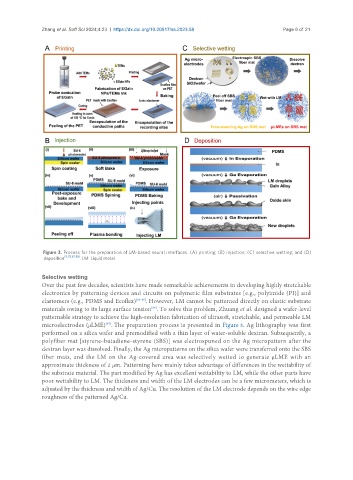
Figure 3. Process for the preparation of LM-based neural interfaces. (A) printing; (B) injection; (C) selective wetting; and (D)
[9,78,87,88]
deposition . LM: Liquid metal.
Selective wetting
Over the past few decades, scientists have made remarkable achievements in developing highly stretchable
electronics by patterning devices and circuits on polymeric film substrates [e.g., polyimide (PI)] and
elastomers (e.g., PDMS and Ecoflex) [82-85] . However, LM cannot be patterned directly on elastic substrate
[86]
materials owing to its large surface tension . To solve this problem, Zhuang et al. designed a wafer-level
patternable strategy to achieve the high-resolution fabrication of ultrasoft, stretchable, and permeable LM
microelectrodes (μLME) . The preparation process is presented in Figure 3. Ag lithography was first
[87]
performed on a silica wafer and premodified with a thin layer of water-soluble dextran. Subsequently, a
polyfiber mat [styrene–butadiene–styrene (SBS)] was electrospuned on the Ag micropattern after the
dextran layer was dissolved. Finally, the Ag micropatterns on the silica wafer were transferred onto the SBS
fiber mats, and the LM on the Ag-covered area was selectively wetted to generate μLME with an
approximate thickness of 2 μm. Patterning here mainly takes advantage of differences in the wettability of
the substrate material. The part modified by Ag has excellent wettability to LM, while the other parts have
poor wettability to LM. The thickness and width of the LM electrodes can be a few micrometers, which is
adjusted by the thickness and width of Ag/Cu. The resolution of the LM electrode depends on the wire edge
roughness of the patterned Ag/Cu.