


Page 25 - Read Online
P. 25
Page 18 of 34                                                Wang et al. Energy Mater. 2026, 6, 600064


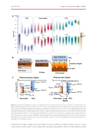
               Figure 4. Schematic band diagrams of energy-level alignment. (A) Energy levels of recently reported CsPbI x Br 3-x  (0 ≤ x ≤ 3) films and
               highly efficient transport layers according to refs [144-149] , which were mainly obtained from absorption spectra and photoelectron
               spectroscopy. Note that the valence and conduction band levels as well as the work function may vary depending on the exact
               stoichiometry but also on the mode of preparation and surface treatments. Reprinted with permission [143] . Copyright 2022, John Wiley and
               Sons. (B) Schematic diagram of PSC without (central panel) and with (right panel) CPS treatment. The open red circles represent V X  sites.
               Reprinted with permission  [150] . Copyright 2021, John Wiley and Sons. (C) Schematic band diagram of perovskite/HTL (i.e.,
               Cs 0.06 FA 0.79 MA 0.15 Pb(I 0.85 Br 0.15 ) 3  and Spiro-OMeTAD) without and with interfacial dipole pointing towards HTL. Note, a rigid energy shift of
               the HOMO and the LUMO of the HTL was assumed caused by the change in E Vac  after CPS treatment. Reprinted with permission [150] .
               Copyright 2021, John Wiley and Sons.


               modulation through a single molecular design strategy. In addition to dipole engineering, the n-type
               characteristics of perovskite can be enhanced by incorporating additive molecules that simultaneously

