
Page 344 - Read Online
P. 344
Page 6 of 11 Zhang et al. Microstructures 2023;3:2023046 https://dx.doi.org/10.20517/microstructures.2023.57
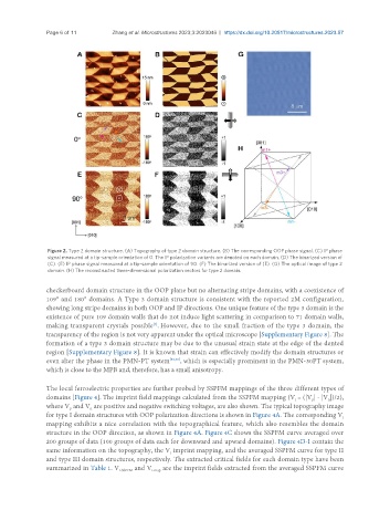
Figure 2. Type 2 domain structure. (A) Topography of type 2 domain structure. (B) The corresponding OOP phase signal. (C) IP phase
signal measured at a tip-sample orientation of 0. The IP polarization variants are denoted on each domain. (D) The binarized version of
(C). (E) IP phase signal measured at a tip-sample orientation of 90. (F) The binarized version of (E). (G) The optical image of type 2
domain. (H) The reconstructed three-dimensional polarization vectors for type 2 domain.
checkerboard domain structure in the OOP plane but no alternating stripe domains, with a coexistence of
109° and 180° domains. A Type 3 domain structure is consistent with the reported 2M configuration,
showing long stripe domains in both OOP and IP directions. One unique feature of the type 3 domain is the
existence of pure 109 domain walls that do not induce light scattering in comparison to 71 domain walls,
making transparent crystals possible . However, due to the small fraction of the type 3 domain, the
[3]
transparency of the region is not very apparent under the optical microscope [Supplementary Figure 8]. The
formation of a type 3 domain structure may be due to the unusual strain state at the edge of the dented
region [Supplementary Figure 8]. It is known that strain can effectively modify the domain structures or
even alter the phase in the PMN-PT system [39,40] , which is especially prominent in the PMN-30PT system,
which is close to the MPB and, therefore, has a small anisotropy.
The local ferroelectric properties are further probed by SSPFM mappings of the three different types of
domains [Figure 4]. The imprint field mappings calculated from the SSPFM mapping (V = (|V | - |V |)/2),
n
i
p
where V and V are positive and negative switching voltages, are also shown. The typical topography image
n
p
for type I domain structures with OOP polarization directions is shown in Figure 4A. The corresponding V i
mapping exhibits a nice correlation with the topographical feature, which also resembles the domain
structure in the OOP direction, as shown in Figure 4A. Figure 4C shows the SSPFM curve averaged over
200 groups of data (100 groups of data each for downward and upward domains). Figure 4D-I contain the
same information on the topography, the V imprint mapping, and the averaged SSPFM curve for type II
i
and type III domain structures, respectively. The extracted critical fields for each domain type have been
summarized in Table 1. V i-SSPFM and V i-map are the imprint fields extracted from the averaged SSPFM curve