
Page 50 - Read Online
P. 50
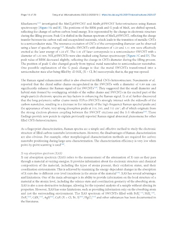
Page 14 of 29        Teng et al. Microstructures 2023;3:2023019  https://dx.doi.org/10.20517/microstructures.2023.07

                          [123]
               Kharlamova  investigated the MnCl @SWCNT and MnBr @SWCNT heterostructures using Raman
                                                                    2
                                                 2
               spectroscopy [Figure 7A and B]. The positions of the RBM peak and G peak of MnX  are shifted upward,
                                                                                        2
               reflecting the change of carbon-carbon bond energy. It is represented by the change in electronic structure
               during the filling process. Peak G is shifted in the Raman spectrum of MnX @SWCNT, reflecting the charge
                                                                              2
               transfer between the carbon wall and encapsulated materials, which leads to the transition of metallic CNTs
               to a semiconductor state. The resonance excitation of CNTs of the corresponding diameter can be observed
               using a laser of specific energy . Metallic SWCNTs with diameters of 1.50 and 1.41 nm were effectively
                                          [123]
               excited at the laser energy of 1.58 eV. The 2.41 eV laser corresponds to a semiconductor SWCNT with a
               diameter of 1.35 nm. NiX @SWCNTs were also studied using Raman spectroscopy [Figure 7C and D]. The
                                     2
               peak value of RBM decreased slightly, reflecting the change in CNTs diameter during the filling process.
               The position of peak G also changed greatly from typical metal nanotubes to semiconductor nanotubes.
               One  possible  explanation  of  the  G  peak  change  is  that  the  metal  SWCNTs  transformed  into  a
               semiconductor state after being filled by 1D NiX  (X = Cl, Br) nanocrystals; that is, the gap was opened.
                                                        2

               The Raman signal enhancement effect is also observed in filled CNTs heterostructure. Nascimento et al.
               reported that the chiral sulfur chains encapsulated in the SWCNTs with a diameter of 0.89 nm can
               significantly enhance the Raman signal of the SWCNTs . They suggested that the small diameter and
                                                                [128]
               hybrid state formed by overlapping orbitals of the sulfur chains and SWCNTs in the excited part of the
               single-particle electronic spectra are key factors in enhancing the Raman signal. Li et al. further discovered
               that the long polymeric sulfur chains inside HiPco-SWCNTs strongly interact with the sidewalls of the
               carbon nanotubes, resulting in a decrease in the intensity of the high-frequency Raman spectral peaks and
               the appearance of new, very strong absorption peaks at 319, 395, and 715 cm , all of which originate from
                                                                                 -1
               the strong electron-phonon coupling between the SWCNT excitons and the S-S vibrations . These
                                                                                                 [129]
               findings provide new points to explain previously reported Raman signal abnormal phenomena for other
               filled CNTs heterostructures.

               As a fingerprint characterization, Raman spectra are a simple and effective method to study the electronic
               structure of filled carbon-nanotube heterostructures. However, the disadvantages of Raman characterization
               are also obvious. For example, other morphological characterization methods are required for carbon
               nanotube positioning during large-area characterization. The characterization efficiency is very low when
                                          [126]
               point-by-point scanning is used .
               X-ray absorption spectrum (XAS)
               X-ray absorption spectrum (XAS) refers to the measurement of the attenuation of X-rays as they pass
               through a material at varying energies. It provides information about the electronic structure and chemical
               composition of the material, including the types of atoms present, their oxidation states, and their
               coordination environments. This is achieved by examining the energy-dependent changes in the absorption
                                                                               [130]
               of X-rays due to different core-level transitions in the atoms of the material . XAS has several advantages
               and limitations. One of the main advantages is its ability to provide information on the local structure of a
               material at the atomic level, including the valence state and coordination geometry of the absorbing atom.
               XAS is also a non-destructive technique, allowing for the repeated analysis of a sample without altering its
               properties. However, XAS has some limitations, such as providing information only on the absorbing atom
               and not the surrounding environment. The XAS spectrum of SWCNTs filled with FeX 2 [115] , NiX 2 [124] ,
               ZnX 2 [104] , CdX 2 [116] , AgX , CuX (X = Cl, Br, I) , HgCl 2 [131]  and other substances has been documented in
                                                      [103]
                                   [102]
               the literatures.